
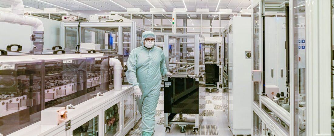
IBM said its Anderon subsidiary has finalized a $1 billion award under the CHIPS and Science Act to advance research and development for U.S.-based quantum wafer manufacturing. The funding is intended to expand the manufacturing foundation needed for quantum processors, a supply-chain issue that could become more important as the technology moves from laboratory work toward commercial systems.
Anderon operates a 300-millimeter quantum wafer foundry in Albany, New York. IBM said it is also backing the venture with an additional $1 billion investment. The company describes Anderon as a pure-play foundry, meaning it offers quantum wafer manufacturing to customers across the quantum ecosystem rather than making processors solely for a single integrated product line.
Quantum hardware requires specialized components and fabrication processes that differ from conventional semiconductor production. According to IBM, Anderon’s wafers support high-performance superconducting qubit arrays, quantum input/output signaling and readout signal-chain components. Those are foundational elements used to build and operate several types of quantum hardware.
The award follows a May letter of intent between the U.S. Department of Commerce and IBM. IBM said Anderon has already run its first quantum wafers through the facility, an early production milestone that the company characterized as evidence it can translate pre-production research into commercial-grade wafer technologies. IBM did not state a timetable for volume production or identify the foundry’s first external customers.
For enterprise technology leaders, the immediate effect will be limited: quantum computing is still an emerging capability rather than a broadly deployed replacement for classical infrastructure. But organizations in sectors with long research, security or optimization cycles have a reason to watch the manufacturing layer as closely as they watch processor roadmaps. A more scalable supply of specialized wafers could affect how quickly quantum hardware providers can prototype, test and eventually build larger systems.
IBM said the foundry will initially focus on superconducting-qubit technology and plans to expand to other quantum modalities in the future. The ability to serve more than one architecture could matter because the industry has not settled on a single dominant approach. Different systems use different physical techniques to create and control qubits, and the supporting components can shape performance, reliability and the path to manufacturing scale.
The company also framed the investment as a domestic-supply-chain effort. A U.S.-based fabrication capability may give quantum hardware developers another option for accessing specialized wafers, while policy makers seek to strengthen local advanced-manufacturing capacity. Whether that produces a meaningful commercial advantage will depend on the foundry’s eventual throughput, technical yields and the needs of potential customers.
IBM cited possible future uses of quantum computing in materials, chemistry, optimization and cybersecurity. Those are long-term possibilities, not current customer outcomes established by the funding agreement. Businesses evaluating quantum technology should distinguish between the new manufacturing investment and deployable computing capacity available today.
Still, the agreement adds a concrete infrastructure development to a field often discussed primarily through research milestones and system roadmaps. The $1 billion award gives Anderon capital for work aimed at production-scale quantum wafer technology. For potential quantum users and suppliers, that is a signal that hardware manufacturing capacity is becoming a strategic part of the ecosystem, alongside advances in processors, error correction and software.